logo
Datasheet4U.com - FDS8962C
logo

FDS8962C Datasheet, MOSFET, Fairchild Semiconductor

FDS8962C Datasheet, MOSFET, Fairchild Semiconductor

FDS8962C

datasheet Download (Size : 700.88KB)

FDS8962C Datasheet
FDS8962C

datasheet Download (Size : 700.88KB)

FDS8962C Datasheet

FDS8962C Features and benefits

FDS8962C Features and benefits


* Q1: N-Channel 7.0A, 30V RDS(on) = 0.030Ω @ VGS = 10V RDS(on) = 0.044Ω @ VGS = 4.5V
* Q2: P-Channel -5A, -30V RDS(on) = 0.052Ω @ VGS = -10V RDS(on) = 0.080Ω @ VG.

FDS8962C Application

FDS8962C Application

where low in-line power loss and fast switching are required.
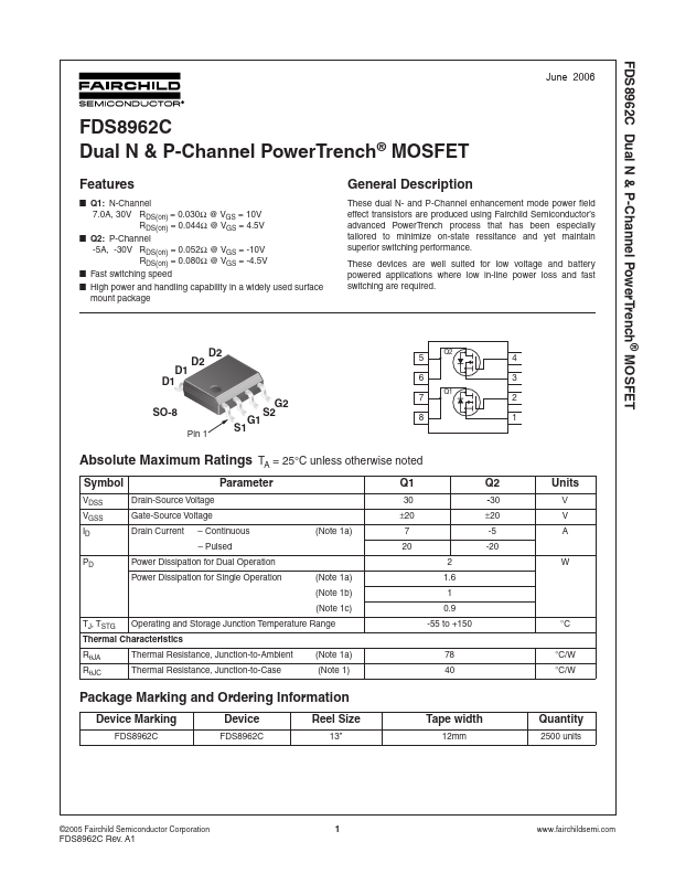
 D1 D1 D2 D2 5 6 Q2 4 3 SO-8 Pin 1 S1 G1 G2 S2 7.

FDS8962C Description

FDS8962C Description

These dual N- and P-Channel enhancement mode power field effect transistors are produced using Fairchild Semiconductor’s advanced PowerTrench process that has been especially tailored to minimize on-state ressitance and yet maintain superior switching.

Image gallery

FDS8962C Page 1 FDS8962C Page 2 FDS8962C Page 3

TAGS

FDS8962C
Dual
P-Channel
PowerTrench
MOSFET
Fairchild Semiconductor

Manufacturer


Fairchild Semiconductor

Related datasheet

FDS8960C

FDS89141

FDS89161

FDS89161LZ

FDS8926A

FDS8928A

FDS8934A

FDS8935

FDS8936A

FDS8936S

FDS8947A

FDS8949

FDS8949-F085

Since 2006. D4U Semicon.   |   Datasheet4U.com   |   Contact Us   |   Privacy Policy   |   Purchase of parts